- 您现在的位置:买卖IC网 > Sheet目录2006 > LTC2755AIUP-16#PBF (Linear Technology)IC DAC 16BIT CUR OUT 64-QFN
LTC2755
17
2755f
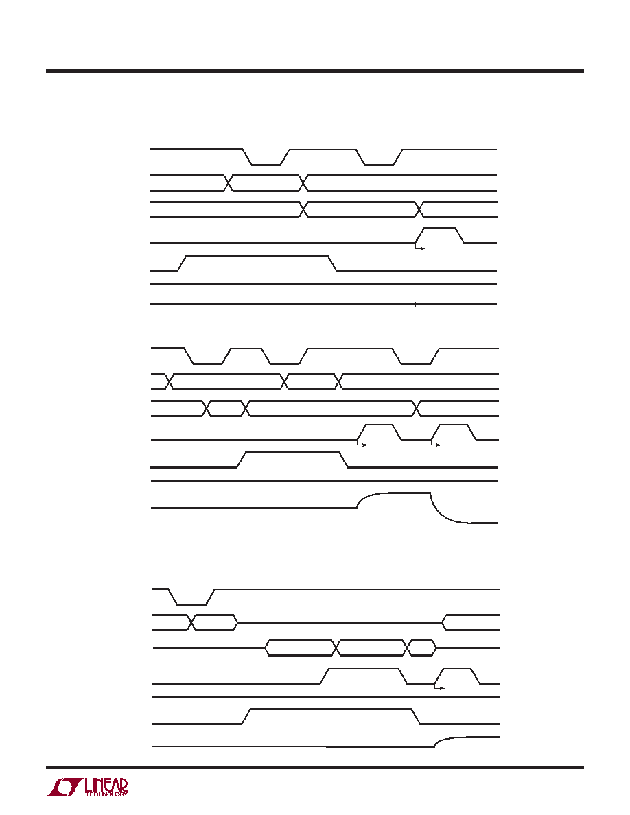
OPERATION—EXAMPLES
WR
SPAN I/O
INPUT
DATA I/O
INPUT
UPD
D/S
8000H
010
READ = LOW
VOUTX
0V (0000H IN 0V TO 5V RANGE)
0V (8000H IN ±5V RANGE)
2755 TD03
UPDATE
(±5V RANGE, VOUT = 0V)
WR
2755 TD04
SPAN I/O
INPUT
DATA I/O
INPUT
READ = LOW
VOUTX
OV
+5V
–5V
UPD
D/S
C000H
4000H
011
UPDATE (5V)
UPDATE (–5V)
WR
2755 TD05
DATA I/O
OUTPUT
DATA I/O
INPUT
READ
UPD
D/S
8000H
0000H
HI-Z
INPUT REGISTER
DAC REGISTER
HI-Z
UPDATE (2.5V)
VOUTX
OV
+2.5V
1. Load ±5V range with the output at 0V. Note that since span and code are updated together, the output, if started at
0V, will stay there. The 16-Bit DAC code is shown in hex for compactness.
2. Load ±10V range with the output at 5V, changing to –5V.
3. Write and update midscale code in 0V to 5V range (VOUT = 2.5V) using readback to check the contents of the input
and DAC registers before updating.
发布紧急采购,3分钟左右您将得到回复。
相关PDF资料
LTC2757ACLX#PBF
IC DAC 18BIT PAR 48LQFP
LTC2758AILX#PBF
IC DAC 18BIT SPI/SRL 48-LQFP
LTC2844IG#TRPBF
IC TXRX 3.3V MULTIPROTCOL 28SSOP
LTC2852MPS#PBF
IC TXRX RS485 20MBPS 14-SOIC
LTC486ISW#TRPBF
IC DVR RS485 LOW PWR QUAD 16SOIC
LTC490IS8#TRPBF
IC TXRX RS485 LOW POWER 8-SOIC
LTC491IS#TRPBF
IC TXRX RS485 LOW POWER 14-SOIC
LTC6900IS5#TR
IC OSC SILICON 20MHZ TSOT23-5
相关代理商/技术参数
LTC2755AIUP-16#TRPBF
功能描述:IC DAC 16BIT CUR OUT 64-QFN RoHS:是 类别:集成电路 (IC) >> 数据采集 - 数模转换器 系列:SoftSpan™ 产品培训模块:Data Converter Fundamentals
DAC Architectures 标准包装:750 系列:- 设置时间:7µs 位数:16 数据接口:并联 转换器数目:1 电压电源:双 ± 功率耗散(最大):100mW 工作温度:0°C ~ 70°C 安装类型:表面贴装 封装/外壳:28-LCC(J 形引线) 供应商设备封装:28-PLCC(11.51x11.51) 包装:带卷 (TR) 输出数目和类型:1 电压,单极;1 电压,双极 采样率(每秒):143k
LTC2755BCUP-16#PBF
功能描述:IC DAC 16BIT CUR OUT 64-QFN RoHS:是 类别:集成电路 (IC) >> 数据采集 - 数模转换器 系列:SoftSpan™ 标准包装:1 系列:- 设置时间:4.5µs 位数:12 数据接口:串行,SPI? 转换器数目:1 电压电源:单电源 功率耗散(最大):- 工作温度:-40°C ~ 125°C 安装类型:表面贴装 封装/外壳:8-SOIC(0.154",3.90mm 宽) 供应商设备封装:8-SOICN 包装:剪切带 (CT) 输出数目和类型:1 电压,单极;1 电压,双极 采样率(每秒):* 其它名称:MCP4921T-E/SNCTMCP4921T-E/SNRCTMCP4921T-E/SNRCT-ND
LTC2755BCUP-16#TRPBF
功能描述:IC DAC 16BIT CUR OUT 64-QFN RoHS:是 类别:集成电路 (IC) >> 数据采集 - 数模转换器 系列:SoftSpan™ 产品培训模块:Data Converter Fundamentals
DAC Architectures 标准包装:750 系列:- 设置时间:7µs 位数:16 数据接口:并联 转换器数目:1 电压电源:双 ± 功率耗散(最大):100mW 工作温度:0°C ~ 70°C 安装类型:表面贴装 封装/外壳:28-LCC(J 形引线) 供应商设备封装:28-PLCC(11.51x11.51) 包装:带卷 (TR) 输出数目和类型:1 电压,单极;1 电压,双极 采样率(每秒):143k
LTC2755BIUP-16#PBF
功能描述:IC DAC 16BIT CUR OUT 64-QFN RoHS:是 类别:集成电路 (IC) >> 数据采集 - 数模转换器 系列:SoftSpan™ 产品培训模块:Data Converter Fundamentals
DAC Architectures 标准包装:750 系列:- 设置时间:7µs 位数:16 数据接口:并联 转换器数目:1 电压电源:双 ± 功率耗散(最大):100mW 工作温度:0°C ~ 70°C 安装类型:表面贴装 封装/外壳:28-LCC(J 形引线) 供应商设备封装:28-PLCC(11.51x11.51) 包装:带卷 (TR) 输出数目和类型:1 电压,单极;1 电压,双极 采样率(每秒):143k
LTC2755BIUP-16#TRPBF
功能描述:IC DAC 16BIT CUR OUT 64-QFN RoHS:是 类别:集成电路 (IC) >> 数据采集 - 数模转换器 系列:SoftSpan™ 产品培训模块:Data Converter Fundamentals
DAC Architectures 标准包装:750 系列:- 设置时间:7µs 位数:16 数据接口:并联 转换器数目:1 电压电源:双 ± 功率耗散(最大):100mW 工作温度:0°C ~ 70°C 安装类型:表面贴装 封装/外壳:28-LCC(J 形引线) 供应商设备封装:28-PLCC(11.51x11.51) 包装:带卷 (TR) 输出数目和类型:1 电压,单极;1 电压,双极 采样率(每秒):143k
LTC2755CUP-12#PBF
功能描述:IC DAC 12BIT CUR OUT 64-QFN RoHS:是 类别:集成电路 (IC) >> 数据采集 - 数模转换器 系列:SoftSpan™ 产品培训模块:Data Converter Fundamentals
DAC Architectures 标准包装:750 系列:- 设置时间:7µs 位数:16 数据接口:并联 转换器数目:1 电压电源:双 ± 功率耗散(最大):100mW 工作温度:0°C ~ 70°C 安装类型:表面贴装 封装/外壳:28-LCC(J 形引线) 供应商设备封装:28-PLCC(11.51x11.51) 包装:带卷 (TR) 输出数目和类型:1 电压,单极;1 电压,双极 采样率(每秒):143k
LTC2755CUP-12#TRPBF
功能描述:IC DAC 12BIT CUR OUT 64-QFN RoHS:是 类别:集成电路 (IC) >> 数据采集 - 数模转换器 系列:SoftSpan™ 标准包装:47 系列:- 设置时间:2µs 位数:14 数据接口:并联 转换器数目:1 电压电源:单电源 功率耗散(最大):55µW 工作温度:-40°C ~ 85°C 安装类型:表面贴装 封装/外壳:28-SSOP(0.209",5.30mm 宽) 供应商设备封装:28-SSOP 包装:管件 输出数目和类型:1 电流,单极;1 电流,双极 采样率(每秒):*
LTC2755CUP-14#PBF
功能描述:IC DAC 14BIT CUR OUT 64-QFN RoHS:是 类别:集成电路 (IC) >> 数据采集 - 数模转换器 系列:SoftSpan™ 产品培训模块:Data Converter Fundamentals
DAC Architectures 标准包装:750 系列:- 设置时间:7µs 位数:16 数据接口:并联 转换器数目:1 电压电源:双 ± 功率耗散(最大):100mW 工作温度:0°C ~ 70°C 安装类型:表面贴装 封装/外壳:28-LCC(J 形引线) 供应商设备封装:28-PLCC(11.51x11.51) 包装:带卷 (TR) 输出数目和类型:1 电压,单极;1 电压,双极 采样率(每秒):143k